
Component family
Ceramic Substrates
Substrates in ceramic for electrical isolation, thermal spreading and mechanical support in power, RF and sensor assemblies.
- Thickness held uniform
- Flatness over the area
- Alignment features located
- Edge condition controlled
A ceramic substrate is a thin, flat component – ground and, where required, laser-cut – that carries an electronic circuit or a thermal path. Aluminum nitride is the usual choice where the part must insulate electrically and conduct heat at the same time. This family covers the ceramic component only: machining, thickness, flatness, surface finish and edge condition. The metallisation, DBC, AMB, thin-film and thick-film processes that follow are carried out by others, and the substrates supplied here are the ceramic carrier for those steps.
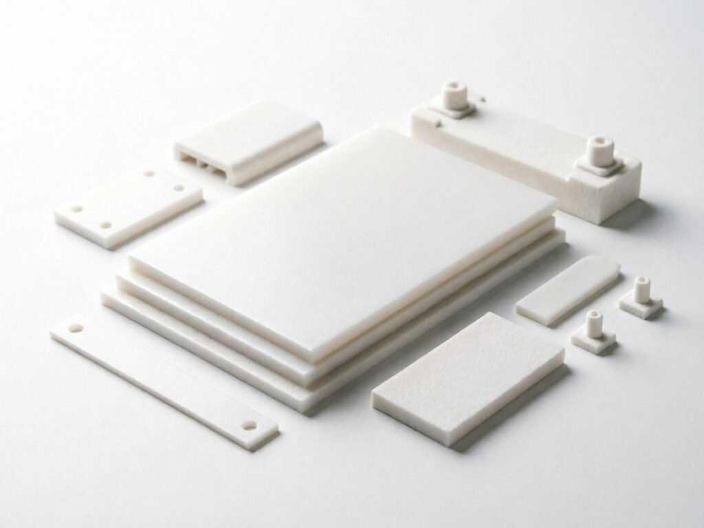
Machined ceramic substrates and thin plates in aluminum nitride, alumina, boron nitride and silicon carbide — thickness, flatness and edges finished to the drawing.
Critical features
What this geometry is judged on
Each row ties one feature to why it matters, where it is at risk in manufacture, and how it is verified. The confirmed figures for these features sit further down the page, tied to the feature they were measured on.
Thickness and uniformity
Ground thin, then measured at several points. Uniformity matters as much as the nominal figure.
Flatness over the functional area
Called out over the area that carries the coating or the bond, not over the whole face.
Surface finish
Specified because the bonding or metallisation step follows from it.
Locating holes and alignment features
Positioned from the datum scheme, because a substrate is usually aligned rather than clamped.
Laser-cut outlines and apertures
Cut from a fired sheet, then checked for kerf width and edge condition.
Edge condition
A chip propagates easily in a thin section, so the edge criterion is agreed with you before production.
| Feature | Why it matters | Manufacturing risk | Inspection method |
|---|---|---|---|
| Thickness and uniformity | Uniformity governs how heat spreads | Grinding thin without breakage | Low-force micrometer at multiple points |
| Flatness over the functional area | The bond or coating follows the face | Controlling flatness after firing and thinning | CMM or optical flat over the functional area |
| Bonding-face finish | Metallisation and bonding follow from it | Keeping the surface free of grinding residue | Stylus profilometer after cleaning |
| Alignment-feature position | The substrate is aligned, not clamped | Locating features on a thin part | CMM or video measurement to the datum scheme |
| Edge condition | A chip propagates in a thin section | Handling thin parts without edge damage | Optical edge inspection per the agreed criterion |
| Kerf width on laser cuts | The cut edge is a functional surface | Keeping a laser edge clean where it meets a ground face | Optical or video measurement of kerf and position |
Possible ceramic materials
Material options and the reason behind each
The material is chosen from the dominant requirement. Where two requirements conflict, the trade-off is explained before quoting.
Combines high thermal conductivity with electrical insulation; the usual choice for power substrates
Aluminum nitride page →Machinable and non-wetting substrate for special thermal paths
Boron nitride page →Where semiconducting behaviour or extreme thermal loading is acceptable
Silicon carbide page →Process routes
How these parts are actually made
The route is chosen from the geometry and the tolerance, not from the material alone. It is stated with the quotation so the price can be read against the method.
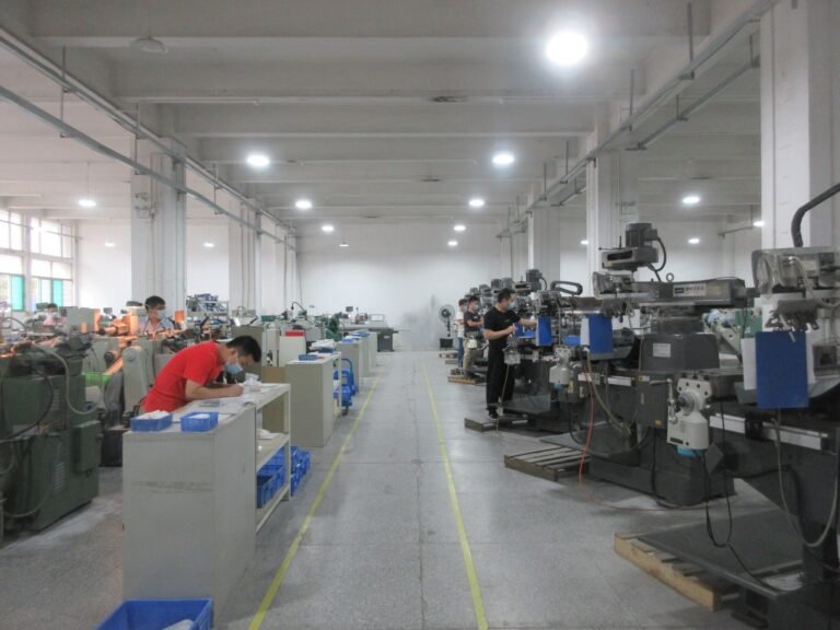
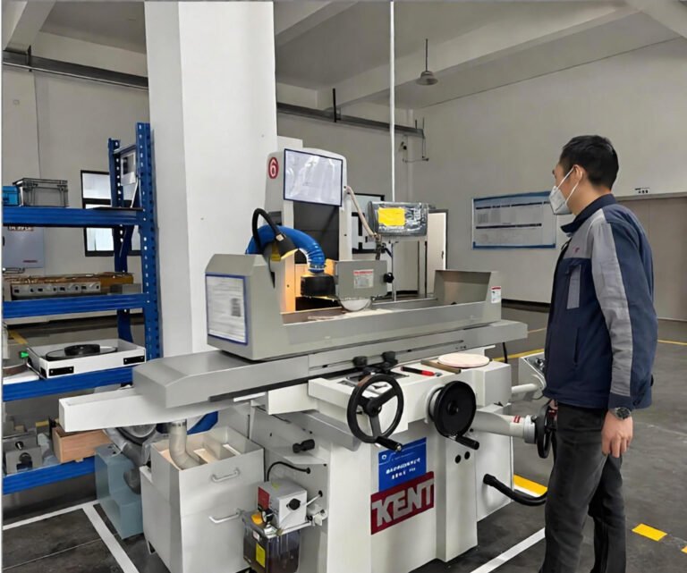
Thin-part grinding
Substrates are ground thin, and handling rather than machining is the limiting factor for the thinnest sections.
Laser cutting of fired substrates
Outlines, apertures and separated arrays are cut by laser from a fired sheet or a near-net blank, so a grinding operation is not needed for every edge. The cut is a defined surface, and the kerf and edge condition are agreed from the drawing rather than left to the process.
Profiling and feature generation
Outline profiles, holes and slots are produced to the drawing, and the achievable edge quality is agreed with the requirement.
Flatness and thickness control
Thickness variation and flatness across the part are inspected because both affect how the substrate sits and how heat spreads.
Where the difficulty sits
- Grinding a thin substrate flat without breaking it
- Holding thickness uniformity across the full area
- Keeping the surface clean and free of grinding residue for thermal paths
- Controlling flatness after firing and after thinning
- Keeping a laser-cut edge clean where it meets a ground face
- Handling and packing very thin parts without edge damage
LimitBrittle material fails differently from metal. A feature that is merely difficult in steel can be impossible in ceramic, and the review states which of the two applies.
Confirmed capability
Customizable geometry and precision capability
Everything below is produced from the customer drawing. The figures are what the shop is confirmed to hold on the features this family carries, not a general tolerance for the whole part.
| Feature | Confirmed | Applies to |
|---|---|---|
| Parallelism | 0.002 mm | Opposed faces of a thin substrate |
| Surface roughness | Ra 0.02 µm | Faces that carry a bond or a metallisation step |
| Hole diameter tolerance | 0.003 mm | Locating and alignment holes |
| Minimum slot width | 0.2 mm | Laser-cut slots and apertures |
Capabilities depend on material, geometry, feature size and finishing requirements. Critical dimensions are reviewed against the drawing.
| Measurement requirement | How it is verified |
|---|---|
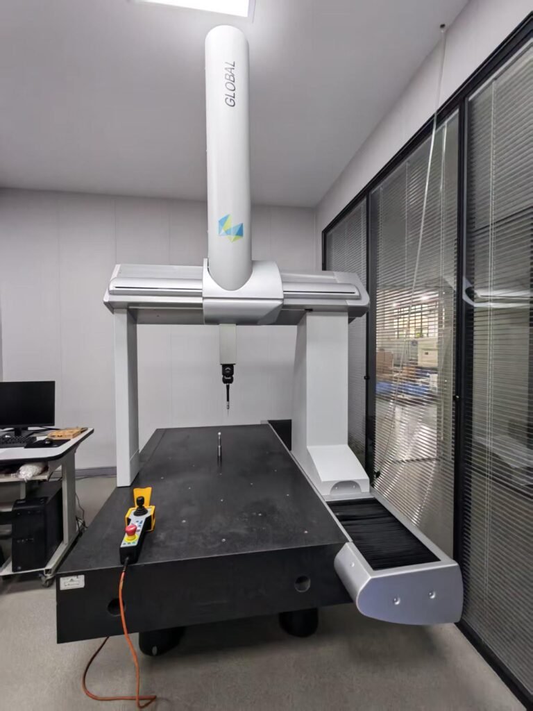
| Thickness and thickness uniformity | Low-force micrometer or thickness gauge at multiple points, because thin parts deform under gauge force |
| Flatness and parallelism over the stated area | CMM or optical flat, with the measurement area following the drawing callout |
| Surface roughness where bonding or metallisation follows | Stylus profilometer on the functional face, after cleaning |
| Position of alignment features | CMM or video measurement against the datum scheme, fixtured without distorting the part |
| Edge quality | Optical edge inspection against the chip criterion agreed before machining |
| Kerf width and position on laser-cut features | Optical or video measurement on the finished edge |
Procurement risks
What goes wrong, and where it is avoided
This family supplies the ceramic carrier only; metallisation, DBC, AMB and thick- or thin-film processing are performed by others.
A chip on a thin edge propagates; the edge criterion is agreed before machining, not at inspection.
Surface cleanliness after grinding affects downstream bonding; the cleaning level is stated with the order.
Thickness uniformity, not just nominal thickness, governs how heat spreads; the uniformity requirement belongs on the drawing.
Applications
Where the family is used
Component examples only. No customer names are published.
- Power module substrates and insulators
- RF and microwave assemblies
- Sensor and detector mounting
- Thermal spreading in dense electronics
- Vacuum and semiconductor equipment hardware
- Electronic ceramic substrates and carrier boards
- Profiled substrates for sensor, RF and detector circuits
- Aluminum nitride substrates for power modules and LED packaging
- Insulating pads and heat-spreading plates
- Thick-film and thin-film substrate carriers
- Laser-cut outlines, apertures and substrates separated from an array
- Vacuum and UHV insulating spacers
Engineering FAQ
Frequently asked
Why aluminum nitride for substrates?
It is one of the few materials that is both a good thermal conductor and an electrical insulator, which is what a power substrate needs. Alumina is cheaper but conducts far less heat.
How thin can a substrate be machined?
Thin sections are produced, but handleability and edge chipping become the limiting factors rather than the grinding process. The achievable thickness is confirmed for the size required.
Are ceramic substrates cut by laser?
Yes. Substrate outlines, apertures and separated arrays are cut by laser from a fired sheet or a near-net blank, which avoids a grinding operation on every edge and allows outlines that grinding alone cannot produce economically. Kerf width and the condition of the cut edge are agreed from the drawing, because in a thin section the cut edge is a functional surface.
Request a quote
Have a Ceramic Substrate Drawing?
Geometry, material, quantity and the dimensions that matter. You get an engineering review before any price is given. Supplying the items below with the drawing removes the most common cause of a revised quotation.
- Thickness with the uniformity requirement stated
- Flatness and which face is the reference
- Surface finish on the bonding or thermal face
- Whether edges must be free of chips and to what criterion
- Which edges are laser cut, with the kerf and edge requirement for those edges
| Type | Form |
|---|---|
| Thin ground discs | and rectangular plates |
| Substrates | with metallisation-ready surface finish |
| Parts | with locating holes, slots or alignment features |
| Stepped and shouldered substrates | locating forms |
| Laser-cut outlines and apertures | cut from a fired sheet |
| Thin sections | with controlled flatness |