
Engineering solution
Vacuum and Semiconductor: Ceramic Components for the Requirement
Outgassing, particle control and plasma exposure in vacuum and semiconductor process equipment, where a polymer part is not an option.
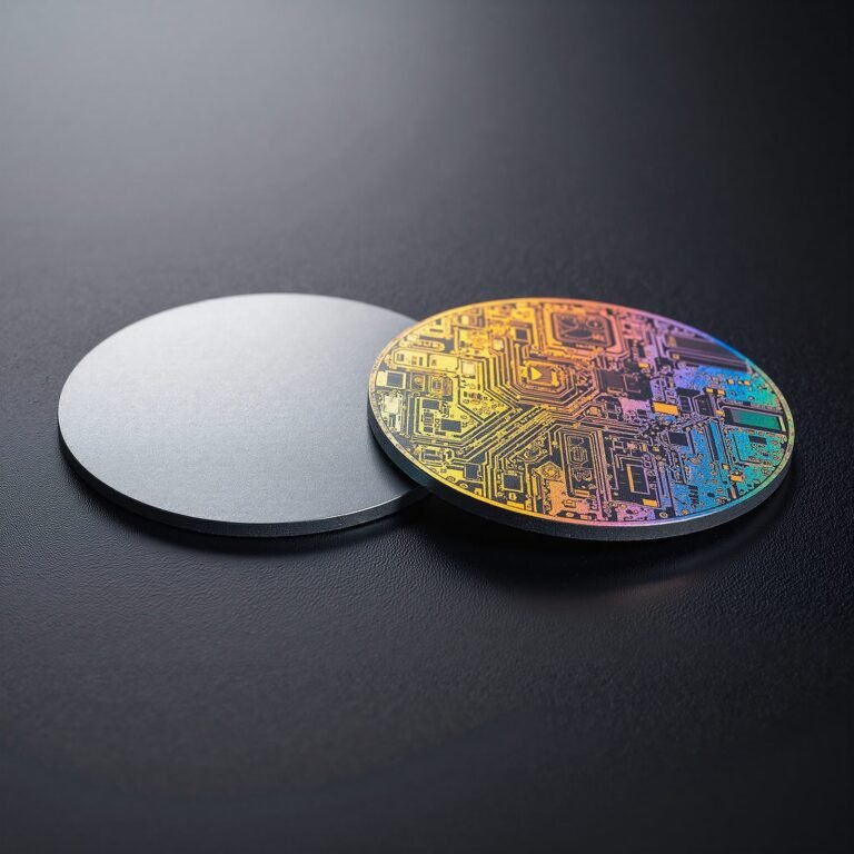
The engineering problem
What is actually failing
A component sits inside a vacuum chamber or a plasma process. Polymers outgas, metals sputter and contaminate, and the part has to survive cleaning and plasma exposure without becoming a particle source.
What the part has to deliver
These are the parameters that decide the material. Not all of them matter equally, which is why the dominant one is identified first.
| Requirement | What it governs |
|---|---|
| Vacuum compatibility | No outgassing and no virtual leaks from trapped volume |
| Particle generation | Edge quality and surface finish that do not shed material |
| Plasma and chemical resistance | Survival in the process gas and cleaning chemistry |
| Thermal behaviour | Tolerance held through process temperature cycling |
| Cleanliness | Suitable for the cleanroom class of the equipment |
Options and the reason behind each
Where two requirements conflict, the trade-off is explained before quoting rather than after.
| Material | Why it is chosen here |
|---|---|
| Alumina (Al2O3) | The standard vacuum insulator; low outgassing and stable under plasma exposure |
| Silicon carbide (SiC) | Plasma-facing and high-temperature components requiring dimensional stability |
| Silicon nitride (Si3N4) | Structural parts inside vacuum equipment under cyclic load |
| Aluminum nitride (AlN) | Vacuum-side insulation where heat must also be removed |
| Boron nitride (BN) | Release and non-wetting surfaces in vacuum and molten metal contact |
What the choice costs in production
These are the constraints that turn a material decision into a manufacturing route, and sometimes into a design change.
- Edge chipping is the dominant defect: a chipped edge in a chamber is a particle source, so the edge criterion is specified
- Blind holes and trapped volumes are avoided or vented to prevent virtual leaks
- Surface finish is controlled to reduce particle retention
- Cleaning after grinding is part of the process, since residue is unacceptable in a process chamber
- Packing must protect edges, because damage in transit has the same effect as damage in machining
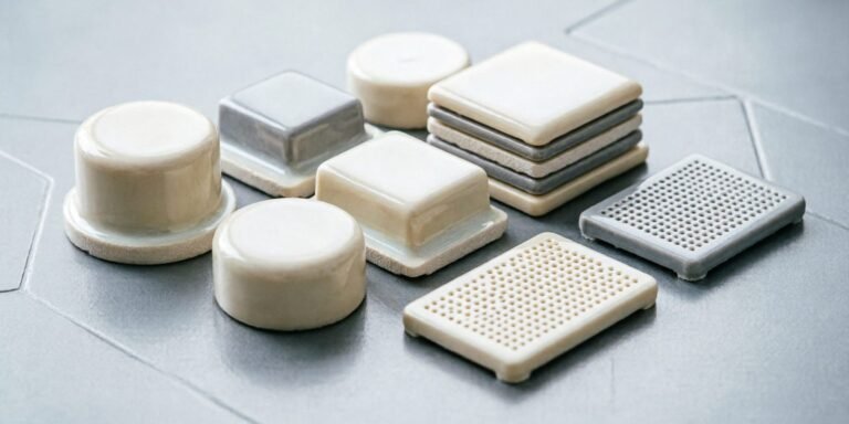
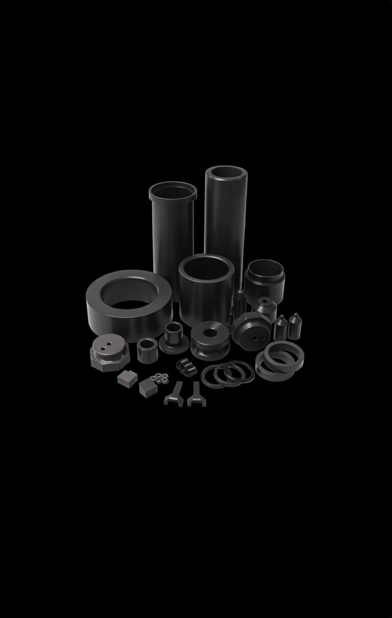
Capabilities depend on material, geometry, feature size and finishing requirements. Critical dimensions are reviewed against the drawing.
Where this solution is applied
Indicative component types. No customer names are published, and no application is described that we have not made.
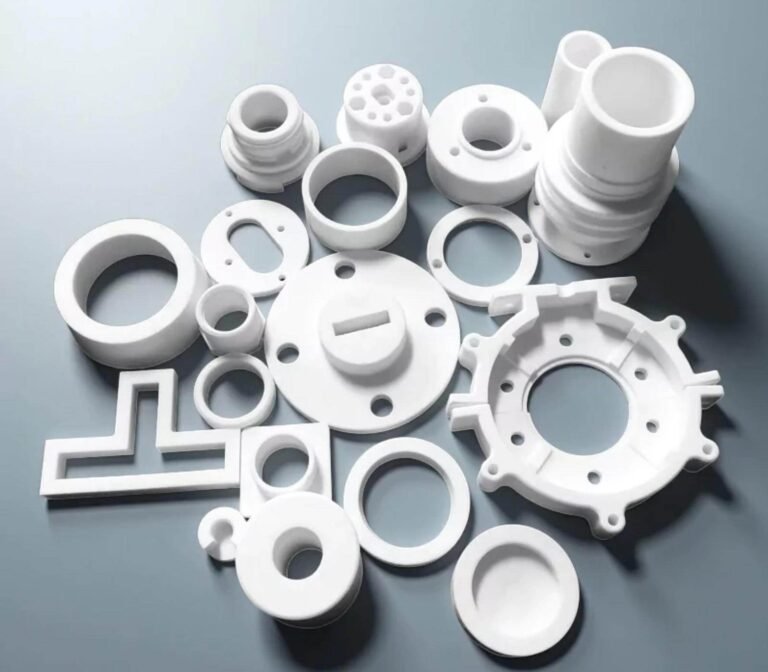
Insulating rings, bushings and standoffs in process chambers
Electrostatic chuck and pedestal components
Gas distribution and flow-restricting parts
Wafer handling contact parts
Vacuum feedthrough and feedthrough insulator bodies
How the result is verified
The inspection plan is agreed before machining, since ceramic cannot be reworked the way metal can.
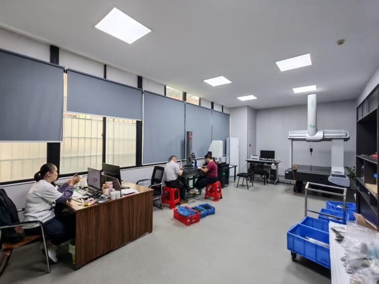
- Dimensional verification of bore and face geometry
- Flatness and parallelism on sealing and mounting faces
- Surface roughness on chamber-facing surfaces
- Optical edge inspection against an agreed chip criterion
- Cleanliness verification and protective packing for transit
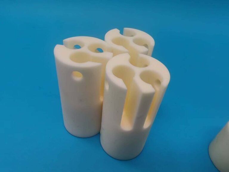
The part and the process
Frequently asked
Describe the problem and send the drawing
The requirement decides the material. Give the conditions and the review will state which material and route apply, and why.