Industry
Semiconductor Equipment: Custom Ceramic Components
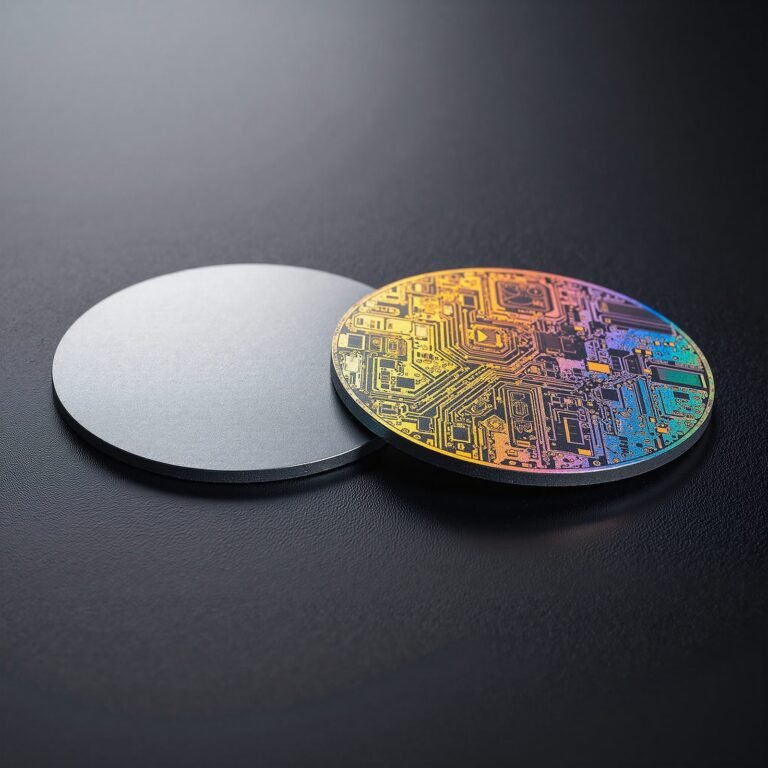
Components inside wafer processing and handling equipment, where a polymer part outgasses in vacuum and a metal part can introduce trace contamination.
Direct answer
What ceramic components does this industry use?
Semiconductor equipment uses precision ceramic components where a polymer part would outgas in vacuum and a metal part could introduce trace contamination. Typical parts are insulating rings, chamber liners, gas distribution components, wafer contact and edge handling parts, and mounting substrates. Alumina covers most insulating duties; silicon carbide and silicon nitride are chosen where a part faces plasma or carries structural load at temperature; aluminum nitride is used where the part also has to remove heat. Suitability is judged against the operating environment stated on the drawing.
Where the parts sit, and what each one does
Each row ties an equipment class to the ceramic component used in it, the function the part performs, the candidate material, the feature that carries the risk and how that feature is verified. Materials named here are the ones described under material selection below.
| Equipment | Ceramic component | Function | Candidate material | Critical feature | Inspection |
|---|---|---|---|---|---|
| Plasma etch and deposition chambers | Insulating rings, chamber liners, gas distribution parts | Isolation of the chamber body from the process, with stable geometry at process temperature | Alumina (Al2O3) as the standard insulator; silicon carbide (SiC) for plasma-facing parts | Wall thickness and bore geometry of the insulating path; edge condition | CMM for position and form; video measurement of apertures and slots; surface roughness on chamber-facing faces |
| Wafer handling and transfer | End effectors, contact and edge handling parts, guide and support parts | Non-contact guidance and wear resistance in vacuum | Alumina (Al2O3); silicon nitride (Si3N4) where the part carries cyclic load | Flatness and parallelism of the contact faces; position of locating features | CMM against the datum scheme; optical edge inspection against an agreed chip criterion |
| Thermal processing | Susceptors, pedestal components, insulating spacers | Dimensional stability through the process temperature range, with insulation | Silicon carbide (SiC) for plasma-facing stability; aluminum nitride (AlN) where heat is also removed | Flatness of seating faces; wall thickness; concentricity of locating features | CMM; surface plate for flatness; thickness measured with a micrometer |
| Metrology and inspection equipment | Reference structures, mounting parts, insulating spacers | A reference geometry that holds position over temperature | Alumina (Al2O3); silicon carbide (SiC) where stiffness matters | Flatness and parallelism; surface finish on the reference face | CMM; video measurement; surface roughness on the reference face |
| Chemical mechanical planarisation | Retaining rings, conditioning components | Wear resistance against a rotating interface, with edge integrity | Alumina (Al2O3); silicon nitride (Si3N4) for cycled mechanical load | Roundness and flatness of the working face; edge condition | Roundness instrument; CMM; optical edge inspection |
Wafer clamps, chuck bodies and lift pins
A wafer clamp sits under a narrower requirement than the handling row above. It is normally a ring, a plate or a pin that contacts the wafer on the edge or the backside, so what the drawing has to fix is the flatness and parallelism of the contact face, the edge condition at the contact radius, and the position of the locating features against the datum scheme. The electrical function of an electrostatic chuck belongs to the equipment design; the ceramic body, plate or ring that carries the wafer is what is machined here, to the geometry and finish stated on the drawing.
Material follows the duty rather than the part name: alumina where the clamp has to insulate, silicon carbide where it faces plasma and wears, silicon nitride where it carries cyclic load, aluminum nitride where heat has to pass through the part into the body behind it. Clamp rings and edge-handling rings are produced as ceramic rings and seals; chuck bodies and seating plates as ceramic plates and blocks; lift pins and guide posts as ceramic shafts and pins. Those pages state the capability figures and the inspection applied to each family, under the same drawing-review caveat used here.
What these parts are judged on
Each row ties one feature to why it matters in service, where it is at risk during manufacture, and how it is measured. The inspection plan is agreed before machining, because a ground ceramic dimension cannot be corrected afterwards.
| Feature | Why it matters | Manufacturing risk | Inspection method |
|---|---|---|---|
| Insulating wall thickness | It sets the electrical path and the stiffness of the part at the same time | Thin walls deflect during machining and chip at the edges | Wall thickness with a micrometer; CMM where the geometry allows |
| Flatness on sealing and mounting faces | A seat that is not flat transfers load unevenly in vacuum service | Holding a large thin face flat while grinding it, and residual stress releasing after machining | Surface plate or CMM across the whole face, not at one point |
| Edge condition inside the process area | A chipped edge becomes a particle source in the chamber | Edge chipping is the most common defect at this scale | Optical edge inspection against an agreed chip criterion |
| Surface finish on chamber-facing faces | Finish limits particle retention and how cleanable the surface is | Reaching the finish without embedding abrasive residue | Surface roughness measurement, with cleaning verified as a process step |
| Concentricity of gas passages and locating features | Flow distribution and alignment depend on those features being on axis | Datum transfer between setups loses concentricity | CMM against the datum scheme |
What the process demands of the material
The conditions below act on the part in service. Each one narrows the material or the geometry, and stating them is what turns the material choice into an engineering decision rather than a preference.
Vacuum
Blind holes and trapped volume become virtual leaks, so they are caught at design review rather than after machining.
Plasma exposure
The surface is exposed for the life of the chamber, so low outgassing and dimensional stability decide the grade, and plasma compatibility is confirmed for the grade specified.
Process temperature
Ceramic stays dimensionally stable through the range, which is what keeps feature positions repeatable.
Electrical insulation
The part insulates by itself, so no additional component is needed in the stack.
Particle contamination
Polymers can outgas in vacuum and metals can sputter under plasma; either one can put trace contamination into the process.
Edge integrity
A chipped edge inside a chamber is a particle source, so the edge criterion is specified rather than assumed.
Which materials suit this industry, and the limits
The material is chosen from the dominant requirement. Where two requirements conflict, the trade-off is explained before quoting rather than resolved silently.
| Material | Why it is chosen here |
|---|---|
| Alumina (Al2O3) | The standard chamber insulator; low-outgassing grades in plasma service, subject to grade qualification |
| Silicon carbide (SiC) | Plasma-facing parts needing dimensional stability at temperature, where grade and process determine compatibility |
| Silicon nitride (Si3N4) | Structural parts under cyclic load inside the chamber |
| Aluminum nitride (AlN) | Vacuum-side insulation where heat has to be removed as well |
Where a chamber component is a first build for a tool that is itself still being qualified, the stages it passes through before the route is frozen are described under prototype to production for ceramic components.
What is controlled and how it is verified
Dimensions and inspection method are agreed before machining, because ceramic cannot be reworked the way metal can.
Dimensions that usually matter
- Bore and face geometry on insulating rings
- Flatness and parallelism on sealing and mounting faces
- Concentricity of gas passages and locating features
- Wall thickness on chamber-facing components
- Slot and aperture width where flow is controlled
Inspection applied
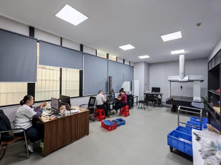
- Coordinate measuring machine for position and form
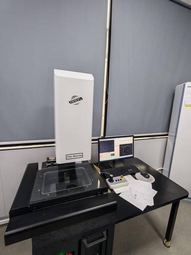
- Optical and video measurement for small apertures and slots
- Surface roughness on chamber-facing faces
- Optical edge inspection against an agreed chip criterion
- Dimensional report, with FAI when a new design is released
Parts made here, on our own equipment
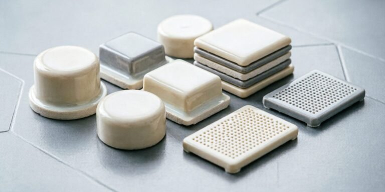
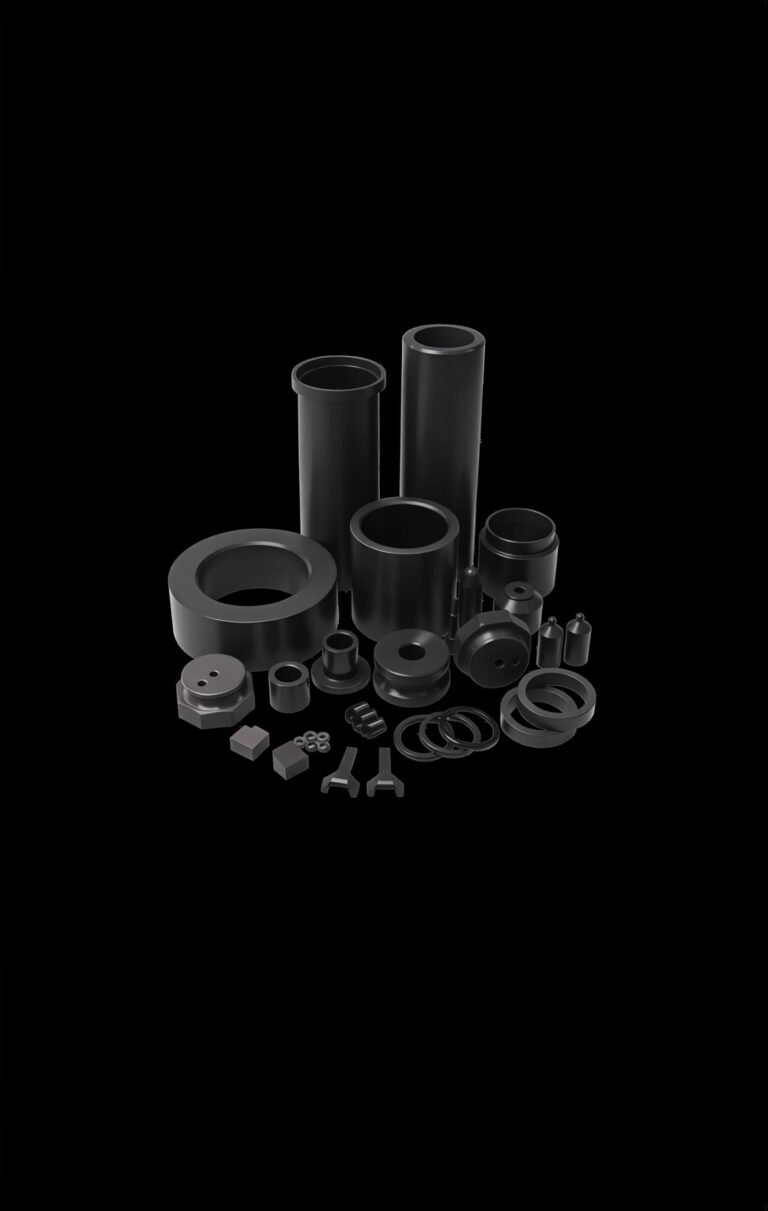
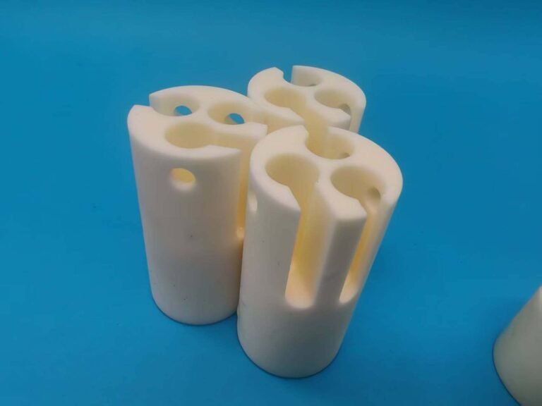
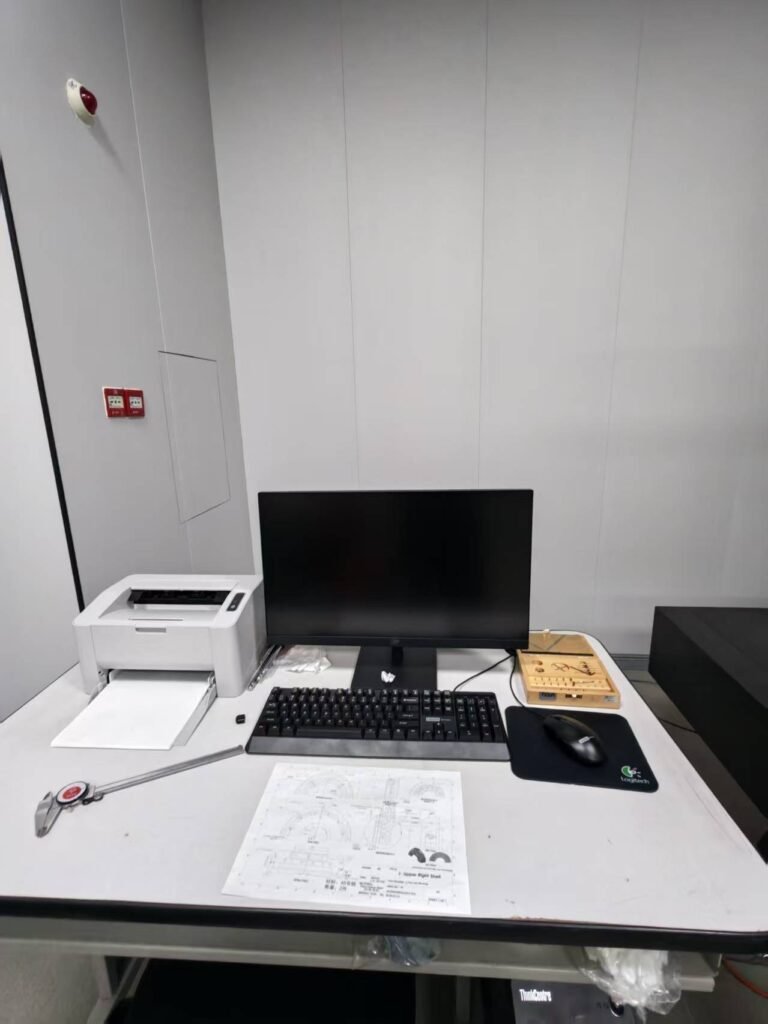
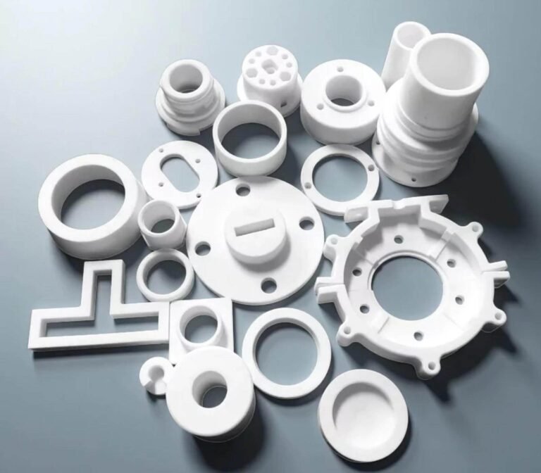
Component photographs are of parts produced in this factory. Equipment photographs are of this plant. No stock photography of facilities we do not own appears on this site.
What to send with a drawing
The review confirms material, route and inspection method from these inputs. Sending them with the drawing is what makes the first quotation accurate.
- Drawing or 3D model, with the datum scheme the part is judged on
- Material or grade if already specified; otherwise the operating environment, including vacuum side, plasma exposure and process temperature
- Critical features and tolerances, in particular insulating wall thickness and flatness
- Quantity at each stage: evaluation, pilot and production
- Surface finish requirement on chamber-facing and sealing faces
- Inspection and documentation needs: dimensional report, first article inspection, material certificate
The part and the process
Frequently asked
Why is ceramic preferred over polymer in a chamber?
Outgassing. A polymer inside a vacuum chamber releases volatiles that can deposit on wafers and change the process. Ceramic grades selected and processed for vacuum service do not release volatiles the way a polymer does.
How is edge quality specified?
Against an agreed chip criterion, stated on the drawing or agreed with the inspection plan. An unspecified edge is the most common cause of disagreement on semiconductor ceramic parts.
Can you supply parts for a chamber that is already in production?
Yes. Send the drawing and, if available, the current inspection method. Parts already qualified in service need the same datum scheme to remain interchangeable.
Do you machine ceramic wafer clamps and wafer handling parts?
Wafer clamps are machined as rings, plates or pins, depending on where the part contacts the wafer. The drawing has to fix the flatness and parallelism of the contact face, the edge condition at the contact radius and the locating features against the datum scheme, because those three decide whether the wafer seats repeatably. Material follows the duty: alumina where the clamp insulates, silicon carbide where it faces plasma, silicon nitride under cyclic load and aluminum nitride where heat has to pass through the part.
Send a drawing for this industry
State the equipment, the operating conditions and the quantities. The review confirms material and route before quoting. Initial engineering feedback is returned within 2 business hours during published business hours (Mon-Fri 9:00-18:00 GMT+8), excluding Chinese statutory holidays and company-announced non-working days; this is initial feedback on the drawing, not completion of a formal quotation or a full engineering review.