Engineering guide
Ceramic Components in Semiconductor Manufacturing
Which ceramic goes into which part of which tool, and why the alternative materials were rejected. Organised as an equipment to component to material mapping rather than as a materials overview.
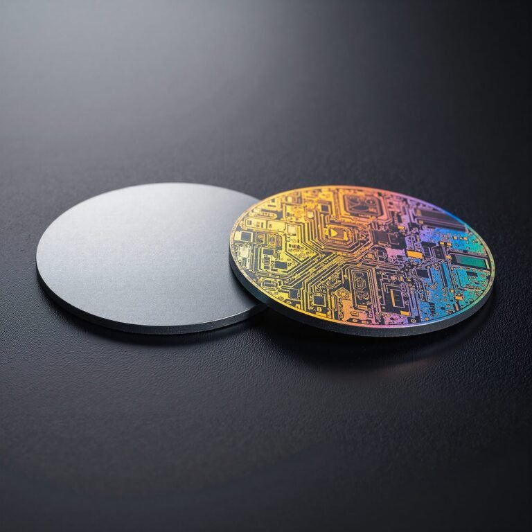
Mapping
Equipment to component to material
| Equipment | Component | Material | Reason |
|---|---|---|---|
| Plasma etch chamber | Insulating ring, liner | Alumina, SiC | No outgassing; survives plasma |
| Deposition chamber | Gas distribution parts | Alumina, SiC | Cleanliness and dimensional stability |
| Wafer handling | Contact and edge parts | Alumina, zirconia | Wear resistance without contamination |
| Thermal processing | Pedestal and spacer components | AlN, SiC | Heat transfer with isolation |
| Metrology | Reference and mounting parts | Alumina, SiC | Thermal stability |
The industry page these parts belong to is semiconductor equipment. The chamber-side requirements that sit on top of the material choice, outgassing and particle control, are worked through under vacuum and semiconductor components.
What the equipment demands
- No outgassing, because volatiles deposit on wafers
- No metallic contamination, which rules out the usual wear materials
- Particle control, which makes edge quality a specification
- Dimensional stability through the process temperature range
- Compatibility with the cleaning chemistry used on the tool
Why edge quality is a functional requirement
A chipped edge inside a chamber is a particle source. This is why the edge criterion is agreed rather than assumed.
Features that have to be caught before machining
| Issue | Why it must be resolved early |
|---|---|
| Blind holes and trapped volume | Virtual leaks in vacuum |
| Sharp edges | Particle generation |
| Surface finish on chamber-facing faces | Particle retention |
| Cleaning access | Residue left in the part |
| Packing design | Transit damage behaves the same as machining damage |
The part and the process
Frequently asked
Why not use a polymer part inside a chamber?
Outgassing. Polymers release volatiles in vacuum that deposit on wafers and change the process.
How is the edge criterion agreed?
It is stated on the drawing or agreed with the inspection plan, along with the method used to verify it.
Can you supply a replacement for a qualified part?
Yes. Send the drawing and, where available, the current inspection method so the datum scheme matches and the part stays interchangeable.
Which material for a plasma-facing component?
Silicon carbide or alumina depending on the plasma conditions and the required electrical behaviour.
Have a drawing that this guide applies to?
Send it with the material and the quantities. The review confirms what is achievable before any price is issued.